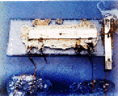
Figure 2: The first monolithic integrated circuit by Jack Kilby, Texas Instruments
The drive for a miniaturization of electronic systems had caused
several attempts to miniaturize conventional components in the
1950s. These attempts were largely unsuccessful, but they illustrated
the demand and potential market for some form of microelectronics.
In 1958, Jack St. Clair Kilby of Texas Instruments, introduced the monolithical
integrated circuit [7]. A semiconductor device was
mounted in a hermetically sealed unit together with resistors and
capacitors constituting an electronic circuit. The connections
between the various components were made by soldering leads to
tiny wires internally. However, the significance of Kilby's
original invention was soon put into the shade by the
almost simultaneous, independent developments at Fairchild Semiconductor.
The invention of the bipolar transistor incited new research into the further exploitation of the characteristics of the semiconductor. The body resistance of the semiconductor and the pn junction capacitance combined with transistors could be combined in the same material to realize a complete circuit, an integrated circuit. Several technology developments6) were required before this potential could be realized.
At Fairchild Semiconductor, a company founded in 1957, a team of research scientists focussed their research efforts on silicon planar technology7). In 1958, Robert N. Noyce developed the planar junction field-effect transistor [10]. The same year, Jean A. Hoerni developed the planar surface field-effect transistor. In this structure, a thin layer of silicon dioxide was used to insulate the gate from the channel of the transistor. The insulating oxide permitted the use of metal lines placed directly on top of the oxide to be used for interconnecting between components.
The process opened the path for the development of the planar technology [9] by Gordon E. Moore and Robert N. Noyce in 1959. In this technology, all components of the IC are incorporated into the same monolithical structure8), and the separation and interconnection of transistors and other circuit elements is done electrically rather than physically using reverse-biased pn junctions. The era of the IC was inaugurated.
The planar technology combines the advantages of junction formation by solid-state diffusion and the masking property of silicon dioxide for precise definition of device geometry. Device geometries are transferred to the wafer using photolithography. Actually, planar processing technology derives its success from the properties of thermally grown silicon dioxide.
Further, planar technology makes use of the important fact that the electrical characteristics of a silicon surface covered with an oxide layer are superior to those of a bare surface. Due to this feature, the sensitivity of semiconductor devices to their environments has been greatly reduced with a corresponding increase in the reproducability and stability of device characteristics.
The final step in the development is to replace bipolar transistors by MOS field-effect transistors (MOSFET)9). In 1960, Martin M. Atalla of Fairchild demonstrates the first MOS field-effect transistor [1]. A few years later, the first commercially available CMOS IC is available [13].
The first consumer product containing IC's was a hearing aid developed jointly by Zenith Radio Corporation and Texas Instruments introduced on 14 February, 1964. From the same period, pMOS technology ICs were used for applications such as calculators. In the late 1960's, the technology shifted to the inherently faster nMOS technology.
The complexity of the manufacturing process delayed the full exploitation
of the CMOS technology for almost twenty years. Today, CMOS technology has
become the dominant VLSI technology.
Author:
Flemming Stassen
(http://www.it.dtu.dk/~stassen/Edu/49260/Historie)