|
|
|
by Bilal K. Taherkheli, Christian P. Kjeldsen,
Asger Stenberg, and Felipe Rivera |
|
|
|
Autumn 2002, 02208 Test of Integrated Circuits |
|
|
|
|
|
Test objectives and DFT strategies |
|
Using IEEE 1149.1 Boundary Scan |
|
IEEE P1500 standard |
|
Structural delay paths and functionally testable
paths |
|
|
|
|
|
|
|
Better functional testability |
|
Increase the quality of functional verification |
|
Easier to test performance requirements |
|
Other factors |
|
Faster and better post fabrication tests |
|
Higher quality ICs |
|
Improve company reputation |
|
|
|
|
|
Low cost |
|
minimal area, 5 sec test time max, cheap ATE |
|
Consistent methodology |
|
Reuse for future products |
|
Automation |
|
ATPG, ATE, use of existing tools |
|
Accountability |
|
Measure fault coverage, specifications |
|
|
|
|
Particular to the characteristics of the design |
|
They, obviously, comply with the defined
objectives |
|
The test engineer chooses among many
alternatives from the IC testing field |
|
|
|
|
|
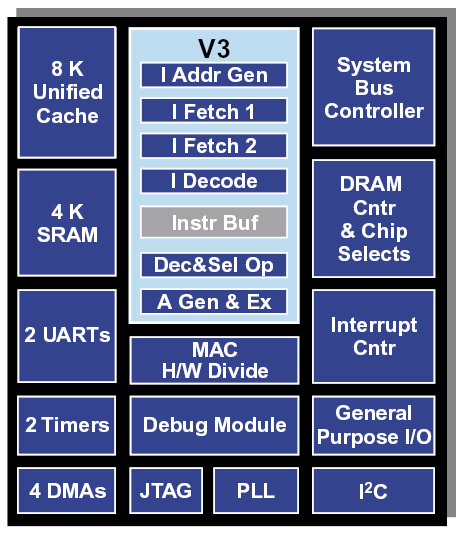
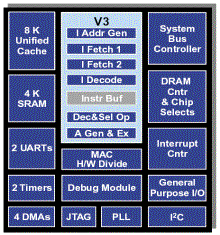
Core |
|
RISC Processor |
|
Embedded memory |
|
Peripherals |
|
All embedded cores portable and synthesizable |
|
|
|
|
|
|
Based on the work for ColdFire V2 |
|
Reused strategies |
|
Path delay testing, At-speed scan, Iddq,
Scan-based burn-in |
|
Some others dropped in favor of better ones |
|
DMA-based memory testing -> MemoryBIST |
|
Some others gone |
|
Sequential testing |
|
New design -> New features -> New
strategies … New Challenges! |
|
Two clock domains |
|
Internal PLL |
|
Doubly embedded nature of the core memory |
|
|
|
|
|
|
Two clock domain |
|
Core at full speed (fastclk), peripherals at
fastclk/2 |
|
ATE, I/O pads, ATPG limitations |
|
Patterns from ATPG had to be post-processed |
|
ATE pin multiplexing |
|
Clock skew |
|
Clock-Data races |
|
Scan testing problems |
|
|
|
|
|
|
|
|
|
V2 DMA-based testing Big interface |
|
Design dependent |
|
No possible to test the SRAM completely |
|
Path delay couldn’t be performed completely |
|
|
|
V3 MemoryBIST |
|
Big area (4%) |
|
More benefits than drawbacks |
|
Core encapsulation |
|
Retention test mechanism |
|
Scan testing of the I/O (Flow-Through RAMs) |
|
|
|
|
|
|
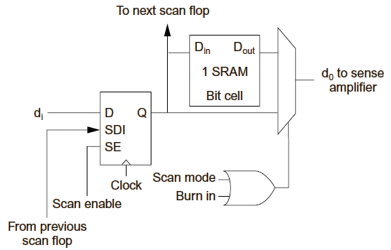
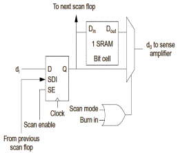
MemoryBIST |
|
Two pauses for retention testing (instead of
six) |
|
Only tests memory cells so there needs to be
additional logic to (flow-through memory) |
|
Test inputs for stuck-at and path delay faults |
|
Test outputs for stuck-at and transition faults
and path sensitization for path delay testing |
|
|
|
|
Testing objectives for embedded microprocessors
can be reached with existing techniques |
|
Time-to-market and economics are the driving
forces behind the defined objectives |
|
A migration path to cheaper ATEs is a
requirement |
|
New challenges for testing arise when different
clock domains are used |
|
|
|
|
What your mother didn’t want you to know |
|
|
|
|
|
Test architecture |
|
Provide access and control to DFT structures |
|
Internal scan, boundary scan, BIST, Emulation
features |
|
Popular on stand-alone IC’s |
|
Low pin count, versatile, easy to comply,
flexible. |
|
Only ONE TAP per IC. |
|
Components |
|
TAP Controller, IR (Indicates what test to
perform), Data registers (test output data) |
|
|
|
|
|
|
|
|
|
|
|
Technical limitations |
|
Can’t apply it to SoC’s due to their modularity |
|
Some IP-Cores have it, some don’t. |
|
JTAG is a separate module, but still tightly
coupled with the core |
|
Breaks the standard |
|
Business and policies |
|
Reluctant to change |
|
Don't see the need |
|
Own policies considered better than the standard |
|
|
|
|
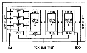
Cores designed to interface to a TAP (TAP1) |
|
TAP’ed cores (TAP2, TAP3, TAP4) |
|
BREAKS the standard |
|
Not optimum |
|
Not good for reuse |
|
Many more AdHoc approaches… |
|
|
|
|
IBM paper proposes a similar solution to allow
the use of existing development tools |
|
Provides consistency in the way multiple IC’s in
a board are currently tested |
|
|
|
|
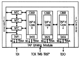
Tap Linking Modules (TLMs) |
|
Standard compliant |
|
Adds a ‘layer’ to isolate the inner
singularities of the modules |
|
G2 PowerPC 603e implements it |
|
Enables background BIST |
|
Still ALL TAPs must be modified and at least one
instruction has to be added |
|
|
|
|
|
Need of a new standard for IP-Core use |
|
P1500 |
|
Another standard |
|
|
|
|
Standard for Embedded Core Test |
|
|
|
|
Yervant Zorian (Chair) |
|
|
|
Erik Jan Marinissen (Chair of Compliance
Definition and Documentation) |
|
|
|
Rohit Kapur (Chair of Core Test Language) |
|
|
|
Maurice Lousberg |
|
|
|
Teressa McLaurin |
|
|
|
Mike Ricchetti |
|
|
|
|
Core Test Language (CTL) |
|
(Worked done in conjunction with the IEEE
1450.6 CTL which is an extension to the IEEE 1450.0 Standard Test Interface
Language (STIL)) |
|
|
|
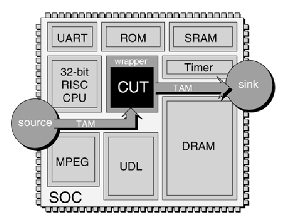
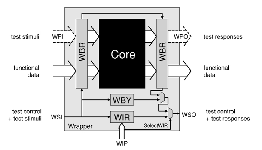
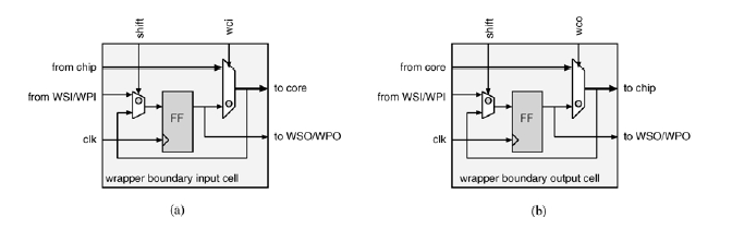
Wrapper |
|
A thin shell around the core, which defines
a standard Core Test Access Point (CTAP) |
|
|
|
TAM : Test Access Mechanism – no longer part of
the IEEE P1500, but it was intended in the beginning. A survey showed that
the testing internal of the Core, and the connections to the test access
mechanism at chip-level was not in demand from the companies. |
|
|
|
|
|
|
Wrapper: |
|
A method to switch between normal, internal
test, and external test mode. |
|
|
|
Only thing considered in this presentation |
|
|
|
|
WSI : Wrapper Serial Input |
|
WSO : Wrapper Serial Output |
|
WIP : Wrapper Interface Port |
|
WIR : Wrapper Instruction register |
|
WBR : Wrapper Boundary Register (made of Wrapper
Boundary Cells) |
|
WBY : Wrapper Bypass Register |
|
WPI : Wrapper Parallel Input (Optional) |
|
WPO : Wrapper Parallel Output (Optional) |
|
|
|
|
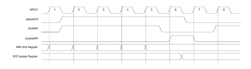
WRCK : Wrapper Clock, dedicated clk for
registers |
|
WRSTN : Wrapper Reset, dedicated active-low
reset signal |
|
SelectWIR : Selects the WIR register when high.
Otherwise either WBR, WBY or any other core-internal register can be chosen
depending on the Instruction. |
|
ShiftWR, UpdateWR, and CaptureWR : Explained on
the next slide. |
|
|
|
|
|
|
ShiftWR : Shifts the wrapper register chosen |
|
UpdateWR : Updates the wrapper register chosen |
|
CaptureWR : What do you think it does? |
|
|
|
So why do we need these three signals? |
|
|
|
|
No FSM as is well-known from IEEE 1149.1 in the
IEEE P1500 |
|
Instead the WIR register is split in two: WIR
Shift Register and WIR Update Register |
|
|
|
|
Normal / Serial Bypass |
|
Serial In Test |
|
Serial Ex Test |
|
Parallel In test |
|
Parallel Ex Test |
|
Others |
|
But I’ll not go through the exact instructions |
|
|
|
|
|
|
Only serial connections of wrappers intended
(i.e. hierarchy is not really supported) |
|
If cores with other Test Access Mechanisms are
used (e.g. JTAG) in combination with the P1500, some functionality is lost. |
|
The connection to a chip level JTAG module not
defined |
|
|
|
|
IEEE P1500 standard meets the stated goal. |
|
However, some people thinks the goals are not
the right ones. |
|
What the standard of the future will be is
uncertain. |
|
|
|
|
|
|
|
PROBLEM |
|
Technology is advancing rapidly with more
transistors per chip and higher operating speeds but tester’s speed is not
increasing at the same rate; affecting delay testing of microprocessors |
|
SOLUTION |
|
An increased trend to employ BIST techniques |
|
|
|
|
|
|
|
Advantages |
|
good test quality |
|
at speed
testing |
|
greater
accuracy than the tester |
|
Disadvantages |
|
increased chip area |
|
reduced
performance |
|
increased design time overhead |
|
higher
power consumption |
|
(non functional random switching) |
|
|
|
|
|
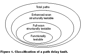
A path is structurally testable if there exists
a test vector pair applied through enhanced or standard full scan chain,
which sensitizes the path. |
|
Enhanced scan structurally testable (all
detectable faults can be tested ) |
|
Full scan structurally testable (not all vector
pairs can be applied) |
|
|
|
|
|
|
|
Do we really NEED all this fancy stuff for
testing a microprocessor? |
|
NO |
|
Functional Test |
|
Use instruction sequences (functional vectors)
as test vectors |
|
Reduced set of test vectors |
|
|
|
|
|
|
|
A path is functionally testable if there exists
a functional test for that path, otherwise its functionally untestable. |
|
A functionally untestable path cannot be tested
by any instruction sequence |
|
Classification of path delay fault |
|
Enhanced scan structurally testable |
|
Full scan structurally testable |
|
Functionally testable |
|
|
|
|
In functional testing certain temporal and
spatial correlations are imposed among registers/flip- flops and thus among
inputs/outputs of the embedded block of the processor |
|
Not all paths are functionally testable even if
they are structurally testable |
|
|
|
|
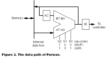
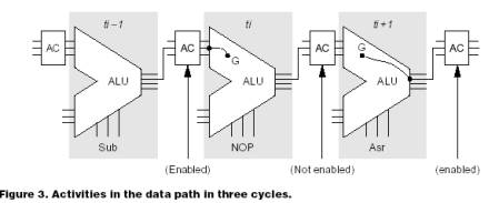
whenever there is a falling transition on S1, AC
and IR can never be enabled in the following cycle |
|
|
|
|
|
|
|
|
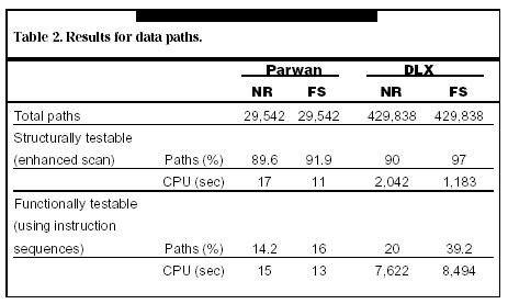
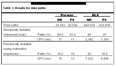
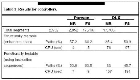
Realistic fault coverage |
|
Reduced test generation effort |
|
Appropriate path selection in delay testing |
|
Identification of true critical paths |
|
Help in
synthesis process |
|
|
|
|
Wow – we are almost finished |
|
|
|
|
Some test objectives have been stated. |
|
A case study of DFT for a microprocessor core
has been made. |
|
The use of IEEE 1149.1 in connection with
embedded cores has been discussed |
|
Parts of the IEEE P1500 has been presented |
|
The use of functionally testable delay paths
over structurally testable delay paths has been addressed |
|
Spend a good deal of your time today |
|
|
|
|
Stassen & Stassen |
|
I test you! |
|

 Noter
Noter