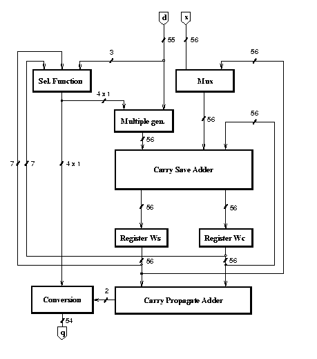
Figure 1: Block diagram of div0 unit
| If you are unable to display correctly math fonts in Netscape under X11, click here. |
ISLPED 96 - International Symposium on Low Power Electronics and Design, Monterey, California. August 12-14, 1996
Alberto Nannarelli and Tomas Lang
LOW-POWER RADIX-4 DIVIDER
Department of Electrical & Computer Engineering
University of California, Irvine, California 92717
e-mail : alberto@ece.uci.edu, tomas@ece.uci.edu
Abstract
The general objective of our work is to develop methods to reduce the
power consumption of arithmetic modules, while maintaining the delay
unchanged and keeping the increase in the area to a minimum.
Here we illustrate some techniques for a radix-4 divider realized in
0.6 mm CMOS technology.
Using techniques such as switching-off not active blocks, retiming the
recurrence, equalizing the paths to reduce glitches, using gates with lower
drive capability, and changing the redundant representation, we obtained a
power consumption reduction of 35% with respect to the standard implementation.
The techniques used here should be
applicable to a variety of arithmetic modules which have similar
characteristics.
1. Introduction
The general objective of our work is to develop methods to reduce the
power consumption of arithmetic modules.
We attempt to reduce the power while maintaining the delay
unchanged and keeping the increase in the area to a minimum.
Since the dynamic power dissipation in CMOS cells
is proportional to the switching frequency and to the
output load [1], we reduce the number of transitions and the
capacitance (by using lower-drive cells when available).
The implementations of the radix-4 divider were done using the COMPASS design environment [2] and the Passport 0.6 mm standard cell library [3]. The structural model was obtained by manually decomposing the behavioral model into functional blocks. Some of those blocks were synthesized by COMPASS from behavioral models to gate networks, others were manually implemented with gates. The power estimation has been carried out with PET [4], a power evaluation tool which computes the power dissipated in a circuit from the netlist extracted from the layout, the standard cell library characteristics, and the results of a logic-level simulation run on a suitable number of test vectors.
Using techniques such as switching-off not active blocks, retiming the recurrence, equalizing the paths to reduce glitches, using gates with lower drive capability, and changing the redundant representation, we obtained a power consumption reduction of 35% with respect to the standard implementation.
In this paper we consider a double precision radix-4 division unit [5], which is typical of those found in many floating-point processors. The recurrence is
w[j+1] = 4w[j] - qj+1d j = 0,1, Ľ28
with the initial value w[0] = x and with the quotient-digit selection
qj+1 = SEL(w[j]7, d3) qj = {-2,-1,0,1,2}
where x the dividend, d the divisor, qj+1 the quotient digit at the j-th iteration and d3 and w[j]7 are the divisor and the residual (carry-save representation) truncated after the 3rd and 7th fractional bit respectively.
We begin with the standard block diagram shown in Figure 1. The recurrence is implemented with the selection function, the multiple generator, the carry-save adder and two registers to store the carry-save representation of the residual W. The conversion block, whose low-power optimization is not treated in this paper, performs the conversion from the signed-digit quotient and performs the rounding using the sign and zero from the carry propagate adder (CPA). The datapath shown in Figure 1 is completed by a controller and by a tree to distribute the clock signal (not depicted in the figure). The corresponding implementation, optimized for minimum delay, has the power dissipation characteristics shown for div0 in Table 3 in the last section.
The resulting block diagram for implementation div2 is shown in Figure 3 (modifications are marked with dotted lines). In this modified divider, the controller selects the input x of the multiplexer during the first cycle and the input d during the rest. In the first cycle, the controller also resets register qj to 1, allowing the input x to be stored in registers W as the first residual w[0].
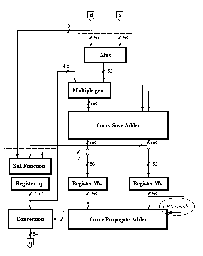
Since now the quotient digit is stored in a register, this has the effect of reducing the glitches in the multiple generator and in the carry-save adder. Also the multiplexer is now out of the recurrence and this reduces the power dissipated in it. The reduction in the number of transitions is 22% and the reduction in power is 16% (with respect to div1).
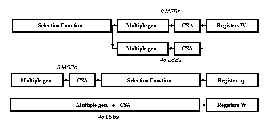
Moreover, now the critical path is limited to the eight most significant bits, so that the forty-eight least significant can be redesigned for lower power dissipation.
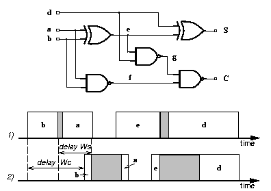
Time diagram 1) in Figure 4 shows the distribution of the arrival times for signal a, b, d, and e. The boxes indicates the range of the arrival times for the 56 bit-slices. This range is produced by the delay in the interconnections; moreover, notice that although a and b both come directly from the registers, a arrives later than b, again because of interconnection delays. In order to eliminate the spurious transitions, we delay the clock to the Ws and Wc registers (which produce a and b) so that the ranges of a and b as well as those of e and d overlap, as shown in time diagram 2) in Figure 4. Anyway, because the regions don't overlap completely, it is impossible to eliminate all the glitches. Moreover, due to the different delays of the XOR and NAND gates, signals at nodes f and g always arrive at different times, and spurious transitions eventually occurring at C, cannot be eliminated either.
Table 1 shows the number of transitions per cycle in the carry-save adder for the two implementations div2 and div3 (where the equalization of paths is applied). With zero-delay transitions we mean the number of transitions in the stationary state, simulating the circuit without delays. Note that in this circuit the number of spurious transitions is a relatively small fraction of the total. The reduction in the number of spurious transitions is 20%.
| zero-delay | actual | spurious | reduction | |
| div2 | 140 | 190 | 50 | - |
| div3 | 140 | 180 | 40 | 10 |
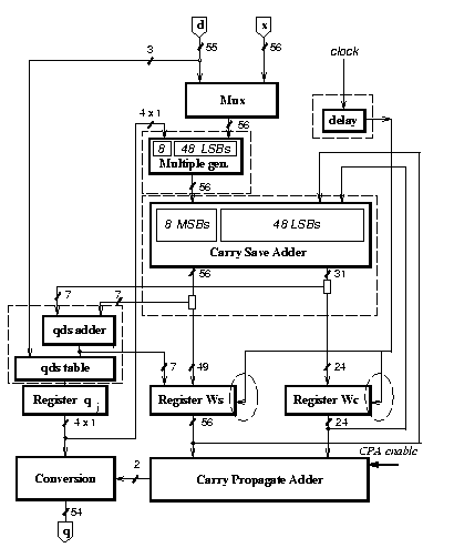
Table 2 shows the reduction in the number of transitions (thousands) for the execution of a division (30 clock cycles) in the different implementations. It also shows the number of transistors (thousands) and area of the dividers.
| div0 | div1 | div2 | div3 | div4 | |
| 0-delay transitions | 17.1 | 13.6 | 11.9 | 11.9 | 9.1 |
| actual transitions | 26.4 | 21.6 | 16.8 | 16.6 | 13.9 |
| no. of transistors | 21.4 | 22.1 | 22.1 | 22.0 | 20.1 |
| Area ( mm2 ) | 1.58 | 1.66 | 1.68 | 1.63 | 1.51 |
Table 3 summarizes the result obtained in the low-power optimization of the divider. Each column represents a different implementation.
| blocks | div0 | div1 | div2 | div3 | div4 |
| control | 0.6 | 0.6 | 0.6 | 0.6 | 0.6 |
| clk tree | 1.9 | 1.9 | 1.9 | 1.9 | 2.1 |
| mux | 0.7 | 0.7 | 0.1 | 0.1 | 0.1 |
| mul. gen. | 2.9 | 2.9 | 1.7 | 1.5 | 1.5 |
| CSA | 5.2 | 5.2 | 3.5 | 2.8 | 2.9 |
| sel. func. | 0.7 | 0.7 | 1.3 | 1.3 | 1.3 |
| register ws | 2.6 | 2.6 | 2.6 | 2.6 | 2.6 |
| register wc | 2.3 | 2.3 | 2.3 | 2.3 | 1.0 |
| register q | - | - | 0.1 | 0.1 | 0.1 |
| CPA | 2.5 | 0.6 | 0.6 | 0.6 | 0.5 |
| Total | 19.4 | 17.5 | 14.7 | 13.8 | 12.7 |
| Ratio | 1.00 | 0.90 | 0.76 | 0.72 | 0.65 |
From Table 3 we conclude that the above mentioned transformations result in an overall power reduction of 35%. The techniques used here should be applicable to a variety of arithmetic modules which have similar characteristics.