|
Copyright 2002 IEEE. To be published in the Proceedings of 2002 IEEE International Symposium on Circuits and Systems (ISCAS), Phoenix, Arizona, USA, May 26-29, 2002.
In the past years, Field Programmable Gate Arrays (FPGA) have gained increasing importance in several areas of VLSI design. Today, FPGAs, which offer a large number of equivalent gates and can be clocked at high frequencies, are becoming a serious competitor of ASICs for some applications. Furthermore, because of the re-configurability, FPGAs provide the quickest approach to system prototyping and a reliable tool to emulate in hardware the behavior of systems too complicated to be simulated in software. For these reasons, it can make sense to extract information on a system by its implementation on FPGAs followed by measurements on the hardware, instead of complicated modeling and long simulation.
In this work, we evaluate the possibility of obtaining power consumption estimates from a FPGA implementation of the system to design. For this purpose, we measure the average power dissipation of circuits mapped on an FPGA, and compare the measurements with the results obtained with software simulation.
Previous work demonstrated that FIR filters implemented in the Residue Number System (RNS) offer better performance of filters realized in the traditional binary system in terms of area and power dissipation [1]. Those results were obtained for the implementation of the filters on standard cells. In this work, we want to verify if consistent results can be obtained for the implementation on FPGA, and comment on the trade-offs between the simulation- estimation and implementation-measurement approaches.
The measurements carried out on the FPGA implementation confirm that RNS filters consumes less power than the corresponding TCS filters.
In [1], we presented the implementation of digital FIR filters
|
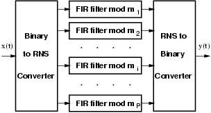
The use of the RNS allows the decomposition of a given dynamic range in slices of smaller range on which the computation can be implemented in parallel [2], [3]. Therefore, a FIR filter can be decomposed, as shown in Figure 1, into P filters of smaller dynamic range (P is the number of moduli) working in parallel. The overhead introduced by the input and output conversions (binary-RNS and RNS-binary) can be reduced by using efficient conversion techniques [4,].
For the implementation of TCS filters, we chose to keep the product in carry-save (CS) format in order to speed-up the operations. The conversion from CS representation to two's complement is performed by a carry-propagate adder (CPA) in the last stage of the filter.
We summarize some of the results of [1] limiting our discussion to the power dissipation of error-free FIR filters realized in transposed form, because they are modular with respect to the number of taps N (i.e. adding extra taps does not alter the filter architecture), and results can be easily extended to any N. In addition, we consider also the implementation of RNS filters which takes advantage of a redundant representation (carry-save) of the residues to reduce the cycle time (e.g. increase the throughput). This scheme, we abbreviate in CS-RNS, is discussed in detail in [6].
For all the filters (TCS, RNS, CS-RNS) we set a 20-bit dynamic range.
In order to cover this range,
we chose for the RNS and CS-RNS filters the following set of moduli
|
|
|
|
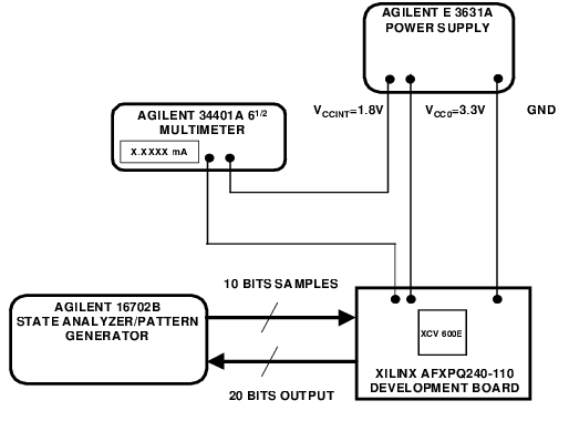
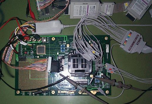
The experimental set-up we used for the characterization of the power consumption in the FPGA is shown in Figure 2. We used the Xilinx AFXPQ240-110 development board equipped with a Virtex V600E HQ240 FPGA [7]. The FPGA can be easily reconfigured by writing directly in its internal RAM or by writing in a 4 Mbit flash memory provided on the board. The programming bit-stream is downloaded from a PC by using the parallel download cable supplied by Xilinx. The development board is equipped with separate power supplies for the FPGA core (VCCINT) and for the I/O banks (VCCO). With this feature, separated measurements of current absorption of the core and of the I/O pads can be easily carried out. The main target of the proposed test bed is the measurement of the core power consumption. Consequently, the mean value of the current absorbed by the core is measured. The different filters under test, have been configured with a low pass frequency mask and have been stimulated by a sequence of random samples (uniform probability density function). The correct behavior of the filters have been checked by acquiring, with the logic state analyzer, the impulse response of the filter. A picture of the Xilinx development board is shown in Figure 4.
 |
The main purpose of the measurements is to evaluate if the expression
of Table 1 found for standard cells are also valid for an
FPGA implementation.
Based on measurements done on FIR filters with a given number of taps,
we want to find an expression for power dissipated in
filters of the same structure with any number of taps. For
this reason, we interpolate the value measured and try to fit a
curve of the type
| (1) |
In order to perform the measurements of average current consumption in the FPGA, we implemented six different filters: 8-tap and 16-tap TCS, 8-tap and 16-tap RNS and 8-tap and 16-tap CS-RNS. All with dynamic range of 20 bits. The VHDL RT-level description of the filters was synthesized and mapped on the FPGA device by using the Xilinx Foundation suite of tools.
Table 2 shows the values of average power dissipation
and area occupation of the different circuits implemented.
The measurements were performed at different clock frequency (Tc).
Average power dissipation was computed from
[`P] = VDD ·[`I], in which VDD is the FPGA
core voltage supply and [`I] is the measured current.
In CMOS, dynamic power dissipation scales with frequency (f = 1/Tc),
but the power
values of Table 2 present some anomalies
due to inaccuracies in the measurement system.
To improve the accuracy of the measurement, we decided to average
the values obtained for different Tc by converting
average power dissipation into energy consumed in a cycle:
|
| (2) |
| |||||||||||||||||||||||||||||||||||||||||||||||||||||||||||||||||||||||||||||||||||||||||||||||||||||||||||||||||||||||||||||||||||||||||||||||||||||||||||||||||||||||||
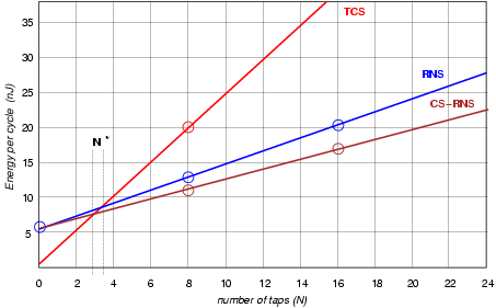
Finally, we fit the average values of Ec for the filters to obtain the expressions of Table 3 and the curves of Figure 3.
From Figure 3 we can see that for filters with more than 4 taps (N* = 4) the RNS filter consumes less power. This result is similar to that of [6] (N* = 4 in Table 1). However, the results of [6] were computed on the synthesized netlist and did not take into account the contribute of interconnections. The value N* obtained here seems to confirm that, due to the small dynamic range of the residues, RNS has shorter (or at least not longer) interconnection wires, and routing is more local of TCS.
The result obtained for CS-RNS filters is even more interesting:
in a standard
cells implementation (Table 1) CS-RNS filters consume
more energy than the corresponding plain RNS filters, while in the FPGA
implementation CS-RNS filters consume less.
In carry-save RNS filters, the modular sum
|
|
 |
In this work, we measured the average power dissipation of FIR filters mapped on an FPGA, and compared the measurements with the results previously obtained for a standard cell implementation. The measurements confirm that RNS filters are smaller and consume less power than the corresponding TCS filters for filters with more than 4 taps. Moreover, the FPGA implementation of the filters in question, seems to be more in favor of RNS, with respect to the standard cells implementation. Carry-save RNS filters offer the best tradeoff delay/area/power for implementations on FPGAs.
Furthermore, we wanted to explore the possibility of carrying out measurements of electrical parameters on hardware to extract information on a system, instead of simulating its behavior with complicated models. The former approach is made possible by the easy, fast and inexpensive re-programmability of FPGAs. Direct measurement requires an initial effort to set-up the measuring environment and to establish a robust testing and measurement methodology. Once the environment is set up, the results are easy to obtain and quite accurate, within the uncertainty of the measuring environment. The advantage of direct measurement is that, no matter how complicated the system under test is, the results are obtained in a short time and with a good accuracy. However, the case of the CS-RNS filter showed that results obtained with FPGAs cannot be extended to standard cells without a careful study of the characteristics of the different technologies and design styles.
In future work, we plan to extend the power analysis of circuits mapped on FPGAs to the measurement of the peak current and the current profile in a clock cycle. At the same time, we are looking into ways of understanding which design style is more appropriate to obtain power savings in circuits mapped on FPGAs.
 |